STM32 Memory Map Series 01: Understanding the 4GB address space and GPIO access
Introduction
Having worked with embedded controllers for some time, a part of the intriguing concepts is the memory arrangement. How does the MCU(microcontroller unit) know where the flash region is? How does the MCU turn an LED on or off? Or how are variables stored in RAM? Ideally, the MCU does not know any of these, it only knows the load instruction(LDR) or store instruction(STR) commands, of course based on its instruction set.
Join me in this series, as we practically debunk these and many other technical facts about STM32 memory arrangement.
Memory map and address space
For a 32-bit MCU like the STM32, there exists a list of possible addresses that the MCU can fetch data from or store data to. The number of addresses depend on the bit-width of the MCU. For a 32-bit MCU/CPU, this value is:
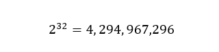
Once we convert this to bytes, we get ~4GB of possible addresses the MCU can address.
Now, the embedded engineer/chip designer comes in and subdivides the 4GB address space into what they want to be accessed once the CPU hits a specific address. Think of it like a street. In a street there are residential houses, shops, factories, reserved plots(not to be accessed ) and the like. So in the 4GB address space, a memory map might look like this one:
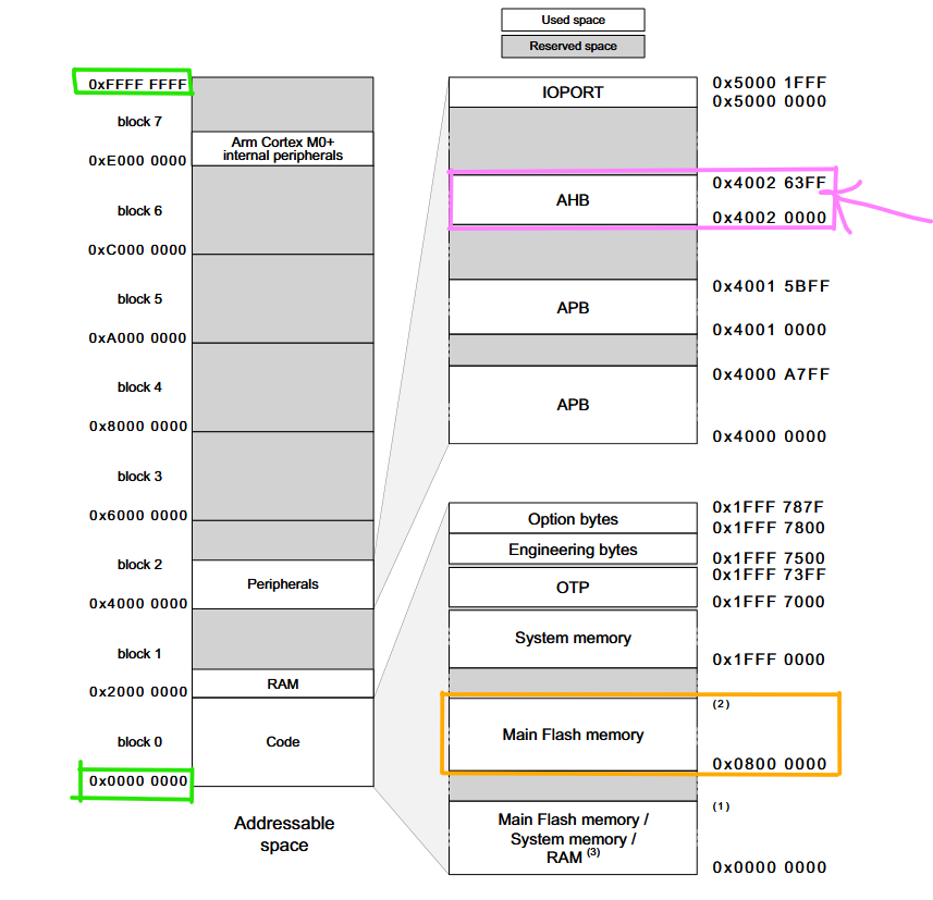
The part labelled in green on the left is the total address range. On the right, you can see the subdivisions of the memory according to function. So the range 0x0800 0000 to 0x1FFF 0000, represents the Main Flash memory region. Therefore, if for example the MCU tries to read a value from a range the address 0x0800 0020, then the region being addressed is the Main Flash memory, where the code is stored, and its is likely to read an instruction.
But how does the MCU know that this is the Main Flash memory? There exists a Bus Matrix whose sole purpose is to route the address to the needed region. The bus matrix is simply the address decoder. I won’t go into all the memory regions in this article.
Memory-mapped IO
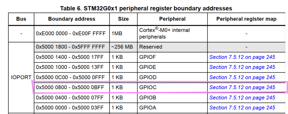
Think about it. If the MCU tries to read/write the address 0x0000 01FF, referring to the memory map above, it will read/write to the RAM, and nothing else happens. However, if we read/write an address at 0x5000 0809, we will access GPIOC, specifically for STM32G0x1 IC, according to the memory map below. By the way, I am using the STM32G0 reference manual, you can find it here: RM0444 reference manual
Now the interesting part is, if you write to a GPIO port, you will toggle the voltage on a pin. For instance for STM32G0, each GPIO port has 10, 32-bit control registers. Namely:
| Name | Offset |
|---|---|
| MODER | 0x00 |
| OTYPER | 0x04 |
| OSPEEDR | 0x08 |
| PUPDR | 0x0C |
| IDR | 0x10 |
| ODR | 0x14 |
| BSRR | 0x18 |
| LCKR | 0x1C |
| AFRL | 0x20 |
| AFRH | 0x24 |
| BRR | 0x28 |
Reference: RM0444 page 245
So, GPIOC_MODER will have an address of 0x5000 0800. If we access this address from the MCU, we can easily get/set the register values. I am not going to describe the function of the registers in this article.
This arrangement of IO registers is called memory-mapping. This is not limited to only the GPIOs, it applies also to other peripherals like UART, TIMERS, ADCs etc.
Memory-mapped register access from C program
Ok. So suppose we want to write the value 0x20 to the output data register(GPIOx_ODR) for GPIOC on STM32G0x1 from our C program. Let us see how to do this.
First, we need to know the base address and ODR register address of GPIOC_ODR.
| Base address | 0x5000 0800 |
|---|---|
| Offset | 0x14 |
| Memory address | 0x5000 0800 + 0x14 = 0x5000 0814 |
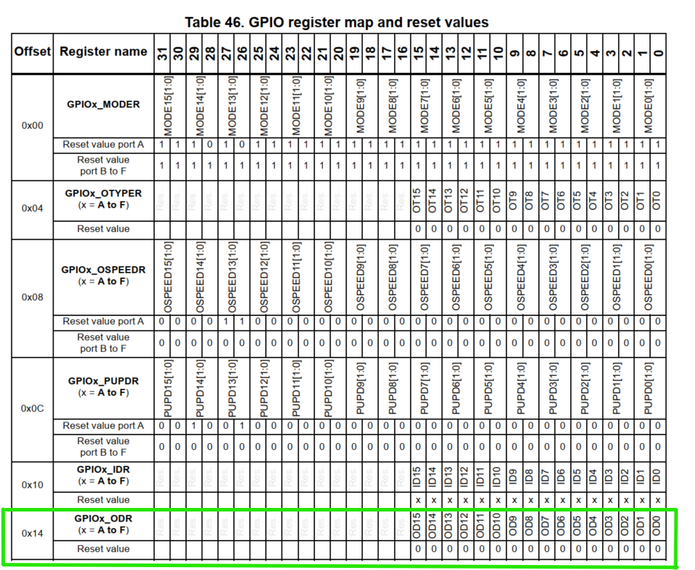
Reference: RM0444 page 245
Now, remember that each register is a 32-bit value. So it means the memory address is a pointer to 32-bit unsigned integer.
We get the value of the GPIOC_ODR as follows:
1
2
3
4
5
#define GPIOC_ODR (*(volatile uint32_t* ) 0x50000814)

{
	GPIOC_ODR |= 0x20; //0b0010 0000 set bit 5 HIGH
}
Breaking this down ins simple statement: Go to address 0x50000814, read what is held in that address, and write the value 0x20 to that address.
In essence, as we will see later, the write is a 3-in-1 step: Read the value in the register, OR 0x20(modify), write back the combined result.
Note that: **
1
*(volatile uint32_t* )* *0x50000814*
is a POINTER TO a register, **it is not the data held in the register, to get the value in that memory location, we dereference the pointer, and write back to ODR.
The volatile keyword is used to prevent the compiler from optimizing your code. Since the GPIO values can change independent of your code, preventing optimization means that the compiler performs the needed operation every time the expression is evaluated, preventing use of stale values.
Since it is manually tedious to refer to every register by hand, CMSIS/ST headers do the following:
1
2
3
4
5
6
7
8
9
10
11
12
13
14
15
16
17
18
19
20
typedef struct {
  volatile uint32_t MODER;    // 0x00
  volatile uint32_t OTYPER;   // 0x04
  volatile uint32_t OSPEEDR;  // 0x08
  volatile uint32_t PUPDR;    // 0x0C
  volatile uint32_t IDR;      // 0x10
  volatile uint32_t ODR;      // 0x14
  volatile uint32_t BSRR;     // 0x18
  volatile uint32_t LCKR;     // 0x1C
  volatile uint32_t AFRL;     // 0x20
  volatile uint32_t AFRH;     // 0x24
  volatile uint32_t BRR;      // 0x28
  /* ... */
} GPIO_TypeDef;

#define GPIOC ((GPIO_TypeDef *)0x50000800)

{
	GPIOC->ODR ^= (1u << 5);   // compiles to an access at 0x50000800 + 0x14
}
Looking at this struct, it is now way easier to access the registers using a base address and a named register. The offsets are calculated automatically, since they are aligned by 4 bytes. Struct members are laid out in order, and each uint32_t takes 4 bytes, so the offsets come out as 0x00, 0x04, 0x08 and so on. This only works because the struct order matches the reference manual exactly. Where the manual has gaps between registers, the headers add RESERVED padding members. We will see this in another article.
Conclusion
Every STM32 program, however how high-level it looks, comes doen to reading and writing numbered locations in a 4GB address space. The memory map is the chip’s fixed plan of what lives at each address: flash, RAM, peripheral registers etc. In the next part we will look at where and how the STM32 stores your code and variables. Stay tuned!