CMOS Image Sensors Explained
Introduction
In my endavour to build a cubesat payload using OV7670 camera, I had to thoroughly understand how this camera module works at the core level, and I thought, why not put this specific part into a blog, that I can later refer to and also anyone interested in the application can read, just for knowledge. So this is it. Enjoy.
In the world of image processing, there is a very key element that aids in the capturing of beautiful images, depending on the application. This element is the camera image sensor. When you think about a camera in its entirity, the only and sole purpose of a camera is to transform moving light into still digital representation that can be saved to memory. The camera in itself is a giant of very clever semiconductor design that has evolved over the years. But it is so minute by design such that it gets very easy to overlook as just another feature.
In this article I am going to debunk the sensor type used in the current market, at the time of writing, without going too technical.
Image Sensing and Acquisition
Just some theoritical background. Light is an electromagnetic radiation that can be sensed by the eye. The wavelength of visible light ranges from apx. 0.43um (violet) to 0.79um (red). Since frequency and wavelength are inversely proportional, violet has a higher frequency than red light. As a matter of fact, to see an object, the wavelength of light reflected by the object must be tha same size or smaller than the size of the object. For example to see water molecules, you need a light source emitting waves at a wavelength less that 10^-10 m, as this is the apx size of a water molecule.
There are may ways to generate images. The most common is obviously energy from electromagnetic waves. However, we can generate images from ultrasonic sound waves, electron beams like used in electron microscopy, and obviously computer generated images.
Acquisition
To acquire an image, all we need is the source of reflected light, which is the object we are trying to capture, and a technology on the sensor that can transform analog quantity to a digitized image. The output voltage waveform is the response of the sensor, and this can then be accurately digitized.
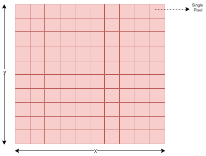
To successfully acquire an image, the geometry has to be in such a way that we can do vertical (y-axis) and horizontal (x-axis) scanning. As a no-brainer, the y-axis creates the vertical pixel array and x-axis creates the horizontal pixel array. The image below shows a basic pixel array:
This illustration shows a great depiction of how an image is produced, of course this is just a very high level depiction:
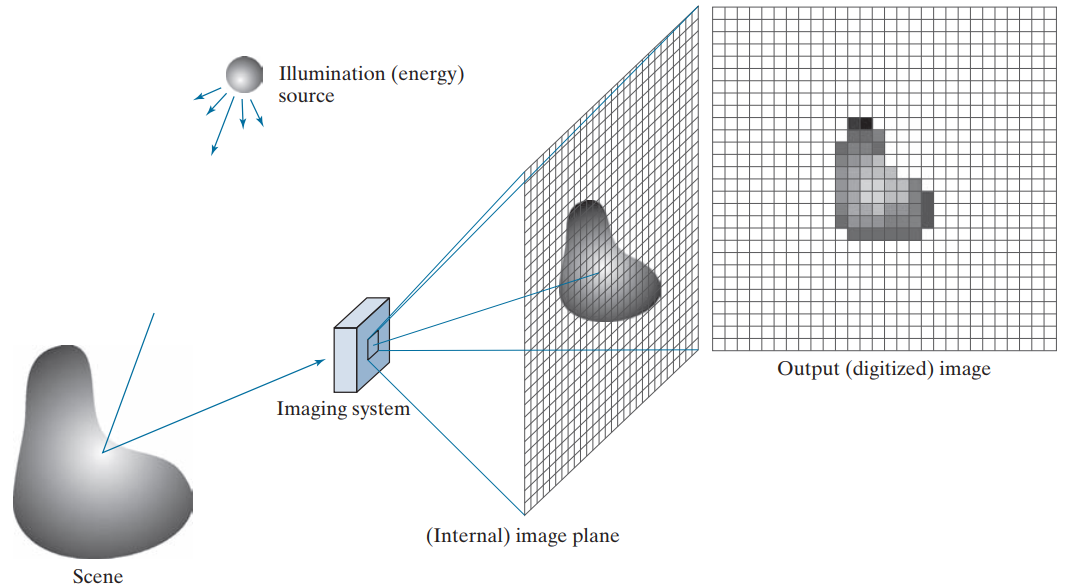 (Source: Gonzales, Woods: Digital Image Processing, 4th Edition)
Types of acquisition sensors
The most popular image capture conversion sensors are CCD and CMOS, though there are may others. CCD stands for Charge-Coupled Device and CMOS stands for Complementary Metal-oxide Semiconductor. A CCD sensor converts incoming photons into electrical charge at each pixel. When a photon hits a pixel, electron-hole pairs are generated. As a result, charge accumulates in each pixel during the exposure. Using clock signals, this charge is shifted across the sensor from pixel to pixel. The charge eventually reaches a readout amplifier which then digitizes the pixel values. CCDs are well-known for an excellent image quality.
Architecture of a 2D CMOS image sensor
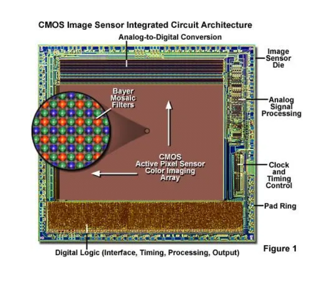
Working Principle of a CMOS sensor
A CMOS sensor is a large array of tiny photodiodes combined with transistor circuitry. The main distintion from CCD is that in CMOS, each pixel has its own processing circuitry. At the heart of the sensor are thousands or millions of individual pixels, depending on the required resolution. Each pixel contains a photodiode, along with transistor circuitry used to reset, buffer and amplify the pixel’s signals. This whole arrangement looks like shown below:
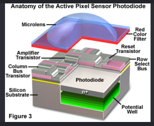
Source: Evident Scientific
When light strikes the pixel, it first passes through a structure known as a microlens. As the job of any lens, the sole purpose of the microlens is to focus and direct incoming light onto the pixel’s photodiode. The reason we need to focus the light is because not the entire area of the pixel is covered by the photodiode, some of it is occupied by the transistors and other circuitry. Without a microlens, light would hit these non-light-sensitive areas and be wasted.
After light passes the microlens, the next most crucial part it has to pass through is the color filter. The most conventional color CMOS image sensors use a Bayer color filter array(CFA), named after Kodak’s Bryce Bayer, who invented this filtering pattern. There is more so much more to this pattern but the most important repeating element in the array is an arrangement of 50% green, 25% red and 25% blue, as shown below:
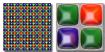
The role of this filter is to give color information to the light reaching the pixel. If a lot of say red light is reaching the pixel, the Bayer array will allow this light to pass through, giving info about the read light. This is ideally where RGB comes from. It is worth noting that there are twice as may green pixels compared to red and blue pixels, simply because human vision registers more luminance around the green spectrum.
This light then reaches the photodiode. There are majorly 2 technologies used in CMOS image sensors, namely photodiodes and photogates. Photogates are beyond the scope of this article. A photodiode is a semiconductor device that converts incident light into a linear output current with respect to the amount of incident light stricking its diode junction. In total darkness, the diode junction has very high resistance and therefore blocks current. Dynamic resistance of the P-N junction inside the photodiode decreases significantly when sufficient light strikes the semiconductor. These photons generate electrons that are then stored inside a potential well.
Finally, we have the transistor circuitry. The transistor circuitry converts the photodiode’s accumulated charge into a usable electrical signal and allows that signal to be read out. There are 4 transistors that are significant .
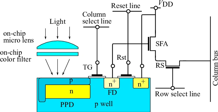
- Transfer transistor - this transfers charge from the photodiode to the floating diffusion node. A diffusion node is a small charge storage region where electrons from the potential well are converted into voltage for readout.
- Reset transistor - resets the floating diffusion to a reference voltage.
- Source-follower transistor - acts as a voltage buffer, converting charge-induced voltage into a signal that can drive the column.
- Row-select transistor - connects that pixel’s signal to the column readout circuitry when its row is selected.
There are some NMOS and PMOS complementary MOSFETS in the circuit, but not all form the CMOS complementary pair. So the broader chip is called CMOS image sensor because it is fabricated using a CMOS semiconductor process.
CMOS adoption
There are other advantages to using CMOS over CCD, but the reason it largely replaced CCD is because it became cheaper, faster and more power efficient, and much easier to integrate with the rest of teh electronic system, as systems evolved into digital. CMOS didn’t simply have a better image quality from the beginning, the advantage is largely architecture and manufacturing process.
A CCD essentially moves charge through the sensor, where the charge from one pixel is transferred to the next until it reaches the output circuitry.CMOS architecture, on the other hand, has an active processing circuitry on each pixel, allowing many signals to be read in parallel, hence making it faster.
In terms of manufacturing process, CMOS image sensors can be manufactured using processes derived from the semicondutor industry that already produces CPUs, memories, digital logic etc. This means that you can put the image sensor and other electronics on the same die, reducing system complexity.
Conclusion
There you have it. A short introduction to some of my learnings from my project. Maybe in another article I will delve into what happens to the image data immediately after it leaves the transistor circuitry, because I kid you not, what happens for you to get a full image is pretty interesting!
Cheers!