STM32 Memory Map Series 02: Into the flash memory
Introduction
Welcome to the second part of this series. Here, I will answer the question, where does the MCU store data in regard to Flash memory. I will debunk the locations of each, significance and their role in an embedded application.
The Flash Memory
Most developers know that flash memory is what stores the code executing on your system. Which is true at a high level. Ideally, it is known as non-volatile memory, that uses the flash technology. Flash technology allows for bulk erasure, random writing, fast read access and dense silicon area implementation, it allows data to be stored even when power is removed.
I will use the reference manual for STM32G0(RM0444) page 61. This is its memory map:
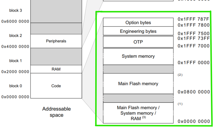
If you look closely, you can see the parts marked (1) and (2). Those the upper boundaries for the specified region. Below the diagram on RM044 there is a caption that I have sourced the below image from:

For a specific IC like the STM32G071xx, the main flash region extends from 0x0800 0000 to 0x0801 FFFF. Doing the math, if you subtract the 2 boundaries you get ~128KB:
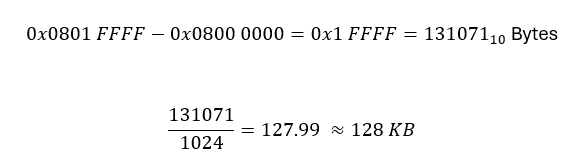
Just as a side note, the STM32G0 gives you an option of having 64KB or 128KB flash memory. For instance the STM32G071C8U6 has 64KB of flash memory. Check ordering guideline for more information on the manufacturer part number.
Flash Memory organization
Ok. So lets say we have this 128KB flash memory. How is it organized. Note that physically, the flash memory is a total of 128KB silicon space on the chip. The flash memory is divided as 72-bit-wide memory cells (64 bits plus 8 ECC bits) that is used to store both code and data constants.
This excerpt from the RM0444 document zooms into the organization.
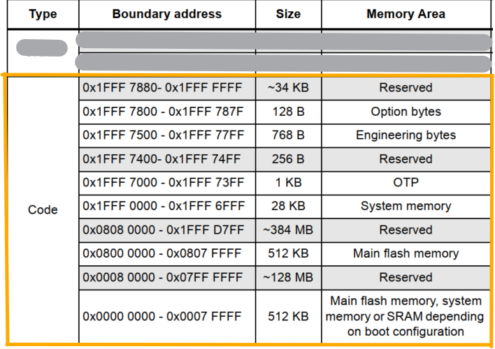
There are 2 major parts of the flash organization from the figure above, the part shown in orange:
- Information block
- Main memory
Information block
Information block spans from 0x1FFF 000 TO 0x1FFF FFFF. This contains regions that hold the system memory(bootloader), OTP(one-time programmable) region, engineering bytes, and the option bytes.
| Region | Purpose |
|---|---|
| System memory(bootloader) | programmed during production. it is used to reprogram the flash memory using either UART, SPI or USB-DFU |
| OTP | 1KB for user data. The OTP can only be written once. It cannot be erased. |
| Engineering bytes | Used in production to hold individual chip’s identity(e.g 96 bit unique device ID) and calibration data. Can be read but you cannot erase them. |
| Option bytes | User configuration |
| Reserved region | RESERVED |
Main memory
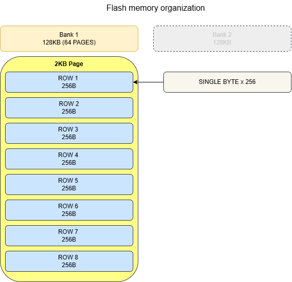
The main memory looks like shown below. The main memory is divided into one or two banks of up to 128 pages of 2KB each, with 8 rows of 256 bytes in each page. The 128KB flash memory has 64 pages. A page in this MCU is the smallest erasable unit.
I will discuss the single-bank devices in this article. Dual-bank will be the subject of another future article.
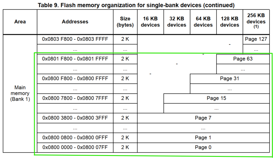
Reference: RM0444 page 72
I have marked the region in green to show our device that has 128KB of flash memory. In terms of pages and banks, this diagram shows the structure:
How code lives inside the main memory
Now that we have the memory map figured out, what is exactly stored in this memory. We know that when you upload code to your MCU, the code remains even after the device is turned off.
Suppose you have the following code block.
1
2
3
4
5
6
7
8
9
10
11
12
13
14
15
const int calibration_value = 100;
int device_status = 1;
int error_count;


int main(void)
{
    int counter = 10;

    while (1)
    {
        counter++;
    }
}
The compiler and linker transforms the source code into binary image containing machine instructions and data. The linker determines where different parts of the program will reside in the MCU’s address space. A compiled code block like the one above contains the following sections:
| Section | Content |
|---|---|
| .isr_vector | Interrupt vector table |
| .text | Executable machine instructions |
| .rodata | Read-only constants and string literals |
| .data | Initialized global and static variables (stored in Flash initially) |
| .bss | Uninitialized or zero-initialized global and static variables |
For instance, callibration_value will be stored as .rodata. device_status is stored initially in flash(.data), then copied into RAM. and error_count is initialized to 0 during startup. These sectors are available in the linker script .ld file after compilation.
How does the MCU run the code
Now that we have some code inside the flash memory region, how do we run it?
In addition to other steps that occur immediately after power up,
- The hardware reads the option bytes from flash at 0x1FFF 7800 into internal registers. For our case, the most significant are nBOOT_SEL, nBTOOT0, and nBOOT1. According to this table, the following are the settings:
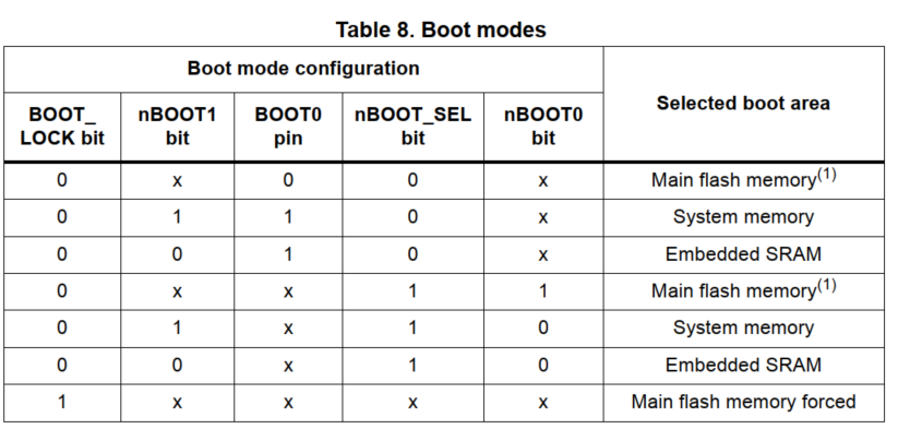
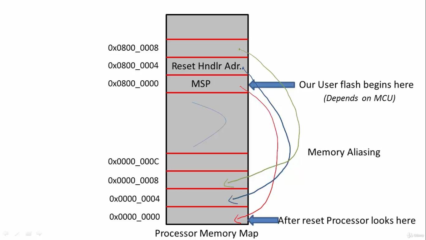
After you release the RESET pin, the Cortex core starts. The core does two mandatory hardwired memory reads. Firstly, it reads the ALIAS address (0x00000000) from the memory map shown earlier. STM32 has several memory regions, but the processor expects by default to find its initial stack pointer and the reset handler at the address 0x0000 0000. Depending on the selected boot mode, STM32 maps(aliases) a different physical memory region into this address(0x0000 0000). This is known as memory aliasing. This is same as having two different addresses that lead to the same storage location.
The mandatory regions that must be read are:
- 0x0000 0000 → Initial main stack pointer(MSP)
- 0x0000 0004 → Reset handler address
In a case where you are booting from main flash memory, these 2 regions are stored in your program’s vector table. So when the processor hits 0x0000 0000, it will redirect to 0x0800 0000 and read the MSP and reset handler.
Your program then executes from its normal flash address and the fetch,decode,execute cycle picks up from there.
Conclusion
This article summarized the STM32 flash memory organization and how the memory map is arranged. However much there is more to write about the flash memory, we will explore them in a later article. I hope gained a little bit more knowledge to help you in your designs. That’s it for now. Good luck!