Anatomy of the OV7670 Camera Sensor
Introduction
Hi there. Been a busy few weeks now. I got stuck on a firmware bug on my cubesat paylod till I sidelined my blog publishing timeline. But now I have made a significant progress on the firmware bug issue, which is related to basically image data transfer from the OV7670 camera to my SD card via DCMI+DMA STM32 channels. Its a pretty interesting development that I will write about soon.
Anyway, this is going to be a fairly short article regarding just the anatomy of the OV7670 camera system that I am using for my payload. If you have been following my cubesat project so far, you know that our payload is designed around the popular 0V7670 camera system from Omnivision. So am going to discuss the parts of this camera and briefly touch on the interfacing to STM32.
This is a purely “theoritical” article, as there will be no code or circuit design whatsoever.
The OV7670 Camera Sensor
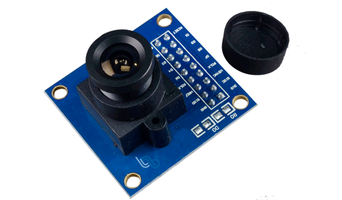
The OV7670 camera sensor/module is a 1/6 inch 0.3-MegaPixel camera that provides the full functionality of a single-chip VGA camera and image processor in a small footprint package (2cmx2cm). What we mean by VGA (Video Graphics Array) in vision technologies is that the resolution of the camera is 640 x 480 pixels.
This camera module has an image array capable of operating at 30fps(frames per second), basically meaning it can capture up to 30 images(frames) in one second, all in the VGA resolution. The upside of this module is that it provides the user with complete control over the image quality, formatting and output data transfer.
Think of a typical camera, maybe your phone’s camera(though pretty advanced). The same way you can control the brightness of an image on the camera, OV7670 gives you this same control of the image qualities such as gamma, exposure control, white balance, color saturation etc, all for a pocket change.
The image below shows this camera:
Working principle
All cameras work in almost pretty the same way.
The lens focuses light onto the image sensor, which is covered by a Bayer color filter pattern. In Bayer patter, each pixel measures only one color component. This will be a discussion for another article, but just to let it out, Bayer arrangement is how a pixel is able to sense a single color (R,G or B), otherwise we would only be sensing the brightness of the color.
The pixel then converts light into charge using photodiode mechanism. During the exposure time, charge will accumulate onto each pixel, with bright areas having more charge and darker areas having less charge. At the end of the exposure, the CMOS image sensor contains a 2D map of charge representing the image.
After this, the OV7670 processor then reads the image row by row. For a VGA resolution, it will read from row 0 to row 479. The read voltage passes through a series of amplifiers to an analog processing stage before it is passed to the image frame buffer.
Since we are dealing with digital systems, this amplified analog values are pased to an analog-to-digital converter to produce a digitized copy of the image frame buffer.
The OV7670 contains a small image processing pipeline that can do neat stuff like auto-exposure, denoising, color processing, auto-whitebalance etc. This is also known as edge image processing (processing at the point of data capture), meaning that your MCU will not have to do a lot of work to clean up the image.
After this, the image can then be passed to the STM32 for processing.
Interfacing
The best way to interface such a huge data chunk (VGA) is to use a parallel method. The camera outputs a parallel line of pixels along side the following elements:
- D0-D7 -> Pixel data
- PCLK -> Pixel Clock
- HREF -> Valid line indicator
- VSYNC -> Valid frame indicator
As you notice, the paralled data (D0 to D7) is 8-bit. Every PCLK edge presents a new byte on D0-D7, which can then be fed into DCMI STM32 channels.
Conclusion
And that’s it for this one. Just a high level view into the OV7670 camera operation, no deep dive. Be on the lookout for the upcoming articles as we disect each part and understand how our cubesat payload interfaces to it.
Cheers!